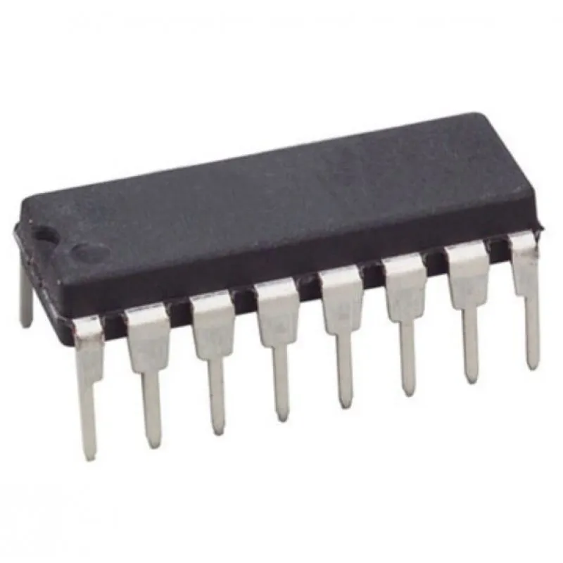
The TL494 device contains two error amplifiers, an on-chip adjustable oscillator, a dead-time control (DTC) comparator, a pulse-steering control flip-flop, a 5-V, 5%-precision regulator, and output-control circuits. The error amplifiers exhibit a common-mode voltage range from –0.3 V to VCC – 2 V. The dead-time control comparator has a fixed offset that provides approximately 5% dead time. The on-chip oscillator can be bypassed by terminating RT to the reference output and providing a saw tooth input to CT, or it can drive the common circuits in synchronous multiple-rail power supplies. The uncommitted output transistors provide either common-emitter or emitter-follower output capability. The TL494 device provides for push-pull or single ended output operation, which can be selected through the output-control function. The architecture of this device prohibits the possibility of either output being pulsed twice during push-pull operation. The TL494C device is characterized for operation from 0°C to 70°C.
Features:-
- Complete PWM Power-Control Circuitry
- Uncommitted Outputs for 200-mA Sink or Source Current
- Output Control Selects Single-Ended or Push-Pull Operation
- Internal Circuitry Prohibits Double Pulse at Either Output
- Variable Dead Time Provides Control Over Total Range
- Internal Regulator Provides a Stable 5-V Reference Supply With 5% Tolerance
- Circuit Architecture Allows Easy Synchronization
Specifications:-
| Symbol | Parameter | Min | Max | Unit |
| VCC | Supply Voltage | 41 | V | |
| VI | Amplifier input voltage | VCC+0.3 | V | |
| VO | Collector output voltage | 41 | V | |
| IO | Collector output current | 250 | mA | |
| Lead temperature 1,6 mm | 260 | °C | ||
| Tstg | Storage temperature range | -65 | 150 | °C |
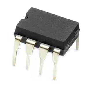
* product image for illustration purposes only. actual product may vary.


There are no reviews yet.