The LF356 device are the first monolithic JFET input operational amplifiers to incorporate well matched, high-voltage JFETs on the same chip with standard bipolar transistors (BI-FET™ Technology). These amplifiers feature low input bias and offset currents/low offset voltage and offset voltage drift, coupled with offset adjust, which does not degrade drift or common-mode rejection. The devices are also designed for high slew rate, wide bandwidth, extremely fast settling time, low voltage and current noise and a low 1/f noise corner.
Features:-
Advantages
- Replace Expensive Hybrid and Module FET Op Amps
- Rugged JFETs Allow Blow-Out Free Handling Compared With MOSFET Input Devices
- Excellent for Low Noise Applications Using Either High or Low Source Impedance
- Very Low 1/f Corner
- Offset Adjust Does Not Degrade Drift or Common-Mode Rejection as in Most Monolithic Amplifiers
- New Output Stage Allows Use of Large Capacitive Loads (5,000 pF) Without Stability Problems
- Internal Compensation and Large Differential Input Voltage Capability
Common Features
- Low Input Bias Current: 30 pA
- Low Input Offset Current: 3 pA
- High Input Impedance: 1012 Ω
- Low Input Noise Current: 0.01 pA/√Hz
- High Common-Mode Rejection Ratio: 100 dB
- Large DC Voltage Gain: 106 dB
Uncommon Features
- Extremely Fast Settling Time to 0.01%: 1.5 μs
- Fast Slew Rate: 12 V/µs
- Wide Gain Bandwidth: 5 MHz
- Low Input Noise Voltage: 12 nV/√Hz
Specification:-
| Parameter | Min | Max | Unit |
| Supply Voltage | ±18 | V | |
| Differential input voltage | ±30 | V | |
| Output short-circuit (to ground) | Continuous | ||
| Operating temperature | -40 | 125 | °C |
| Soldering information (lead temp.) | 260 | °C | |
| Storage temperature | -65 | 150 | °C |
| Input voltage | ±16 | V |
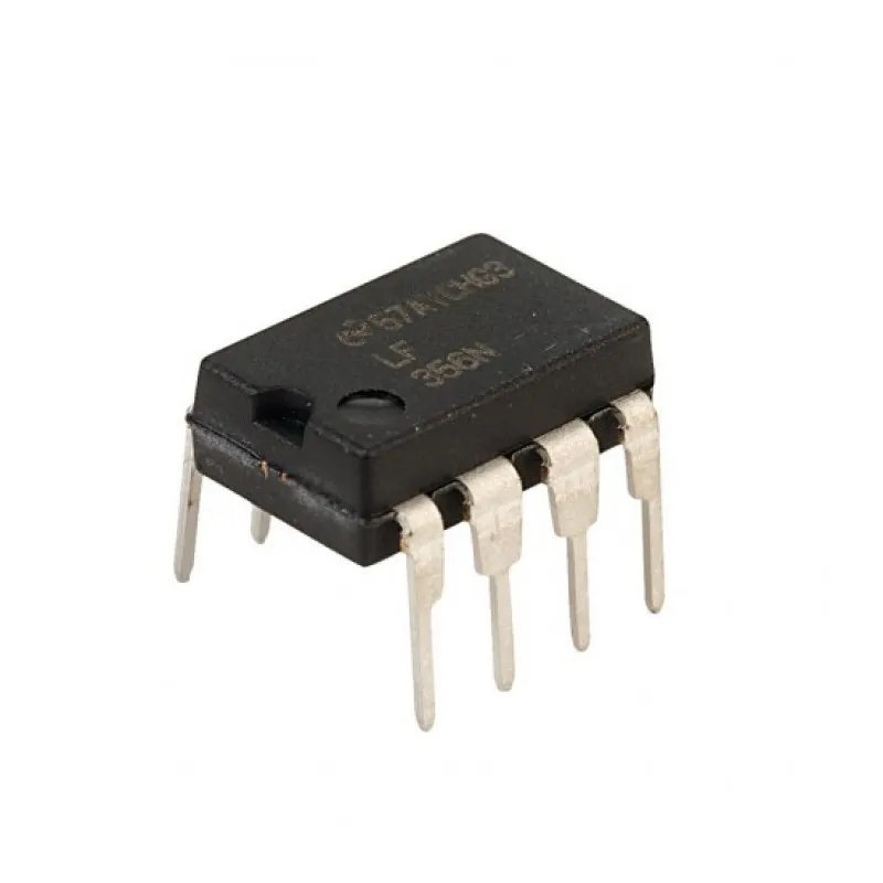
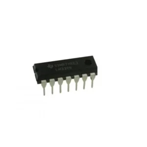
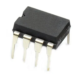
* product image for illustration purposes only. actual product may vary.

There are no reviews yet.