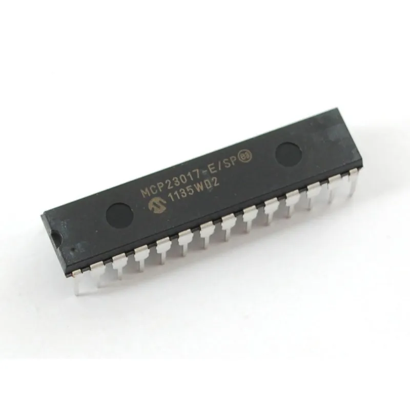
MCP23017 16-Bit Input/Output Expander with I2C Interface IC DIP-28 Package
₹599.00 Excluding tax
The MCP23017 device family provides 16-bit, general purpose parallel I/O expansion for I2C bus or SPI applications. The two devices differ only in the serial interface:
- MCP23017 – I2C interface
The MCP23X17 consists of multiple 8-bit configuration registers for input, output and polarity selection. The system master can enable the I/Os as either inputs or outputs by writing the I/O configuration bits (IODIRA/B). The data for each input or output is kept in the corresponding input or output register. The polarity of the Input Port register can be inverted with the Polarity Inversion register. All registers can be read by the system master. The 16-bit I/O port functionally consists of two 8-bit ports (PORTA and PORTB). The MCP23X17 can be configured to operate in the 8-bit or 16-bit modes via IOCON.BANK. There are two interrupt pins, INTA and INTB, that can be associated with their respective ports, or can be logically OR’ed together so that both pins will activate if either port causes an interrupt.
Features:-
- 16-Bit Remote Bidirectional I/O Port:
- I/O pins default to input
- High-Speed I2C Interface (MCP23017):
- 100 kHz
- 400 kHz
- 1.7 MHz
- Three Hardware Address Pins to Allow Up to Eight Devices On the Bus
- Configurable Interrupt Output Pins:
- Configurable as active-high, active-low or open-drain
- INTA and INTB Can Be Configured to Operate Independently or Together
- Configurable Interrupt Source:
- Interrupt-on-change from configured register defaults or pin changes
- Polarity Inversion Register to Configure the Polarity of the Input Port Data
Specification:-
| Parameter | Value |
| Ambient temperature under bias | -40°C to +125°C |
| Storage temperature | -65°C to +150°C |
| Voltage on VDD with respect to VSS | -0.3V to +5.5V |
| Voltage on all other pins with respect to VSS (except VDD) | . -0.6V to (VDD + 0.6V) |
| Total power dissipation | 700 mW |
| Maximum current out of VSS pin | 150 mA |
| Maximum current into VDD pin | 125 mA |
| Input clamp current, IIK (VI < 0 or VI > VDD) | ±20 mA |
| Output clamp current, IOK (VO < 0 or VO > VDD). | ±20 mA |
| Maximum output current sunk by any output pin | 25 mA |
| Maximum output current sourced by any output pin | 25 mA |
| ESD protection on all pins (HBM:MM | 4 kV:400V |
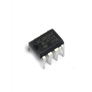
* product image for illustration purposes only. actual product may vary.

There are no reviews yet.