The FAN7392 is a rnonolithic high- and low-sde gate drive IC that can drive high-speed MOSFETs and IGBTs that operate up to +600V. It has a buffered output stage with all NMOS transistors designed for high pulse current driving capability and minimum cross-conduction. Fairch- ild’s high-voltage process and cornnwl-rnode noise can- celing techniques provide stable operation of the high- side driver under high dv/dt noise circumstances. An *Ivanced level-shift circuit offers high-side gate driver operation up to Vs=-9.8V (typical) for VBS=15V. Logic inputs are compatible with standard CMOS or LSTTL output. down to 3.3V logic The I-JVLO circuit prevents malfunction when VCC and VBS are lower than the speci- fied threshold voltage. The high-current and low-output vol* drop feature makes this device suitable for half- and full-bridge inverters, like power Sup- r DC-DC converter applications.
Features:-
- Floating Channel for Bootstrap Operation to +600V
- 3AJ3A Sourcing/Sinking Current Driving Capability
- Common-Mode dv/dt Noise Canceling Circuit
- 3.3V Logic Compatible Separate Logic Supply (VDD) Range from 3.3V to 20V
- Under-Voltage Lockout for vcc and VBS Cycle-by-Cycle Edge-Triggered Shutdown Logic
- Matched Propagation Delay for Both Channels
- Outputs In-phase with Input Signals
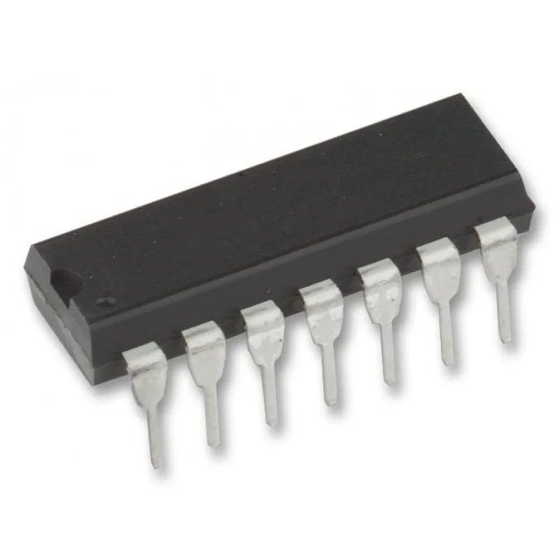
- Available in 14-DIP and 16-SOP (Wide) Packages
Specifications:-
| Parameters | Min | Max | Unit |
| High-Side Floating Supply Voltage-VB | -0.3 | 625 | V |
| High-Side Floating Offset Voltage-VS | VB-25.0 | VB+0.3 | V |
| High-Side Floating Output VoltageVHO | VS-0.3 | VB+0.3 | V |
| Low-Side Supply Voltage-VCC | -0.3 | 25 | V |
| Low-Side Floating Output Voltage-VLO | -0.3 | VCC+0.3 | V |
| Logic Supply Voltage-VDD | -0.3 | VSS+25.0 | V |
| Logic Supply Offset Voltage-VSS | VCC-25.0 | VCC+0.3 | V |
| Logic Input Voltage (HIN, LIN and SD)VIN | VSS-0.3 | VDD+0.3 | V |
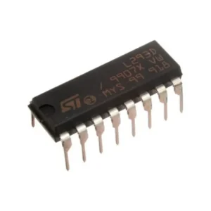
* product image for illustration purposes only. actual product may vary.

There are no reviews yet.