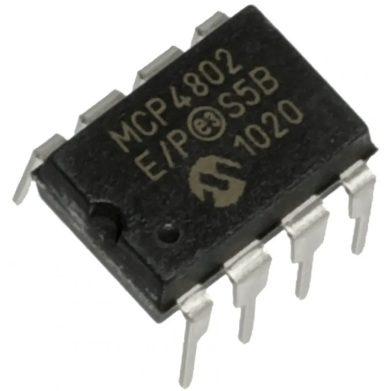
MCP4802 8 Bit Dual Voltage Digital to Analog Converter (DAC) with SPI Interface IC DIP-8 Package
₹199.00 Excluding tax
The MCP4802 devices are dual 8-bit, 10-bit and 12-bit buffered voltage output Digital-to-Analog Converters (DACs), respectively. The devices operate from a single 2.7V to 5.5V supply with SPI compatible Serial Peripheral Interface. The devices have a high precision internal voltage reference (VREF = 2.048V). The user can configure the full-scale range of the device to be 2.048V or 4.096V by setting the Gain Selection Option bit (gain of 1 of 2). Each DAC channel can be operated in Active or Shutdown mode individually by setting the Configuration register bits. In Shutdown mode, most of the internal circuits in the shutdown channel are turned off for power savings and the output amplifier is configured to present a known high resistance output load .
The devices include double-buffered registers, allowing synchronous updates of two DAC outputs using the LDAC pin. These devices also incorporate a Power-on Reset (POR) circuit to ensure reliable powerup. The devices utilize a resistive string architecture, with its inherent advantages of low DNL error, low ratio metric temperature coefficient and fast settling time. These devices are specified over the extended temperature range (+125°C). The devices provide high accuracy and low noise performance for consumer and industrial applications where calibration or compensation of signals (such as temperature, pressure and humidity) are required. The MCP4802 devices are available in the PDIP, SOIC and MSOP packages.
Features:-
- MCP4802 Dual 8-Bit Voltage Output DAC
- Rail-to-Rail Output • SPI Interface with 20 MHz Clock Support
- Simultaneous Latching of the Dual DACs with LDAC pin
- Fast Settling Time of 4.5µs
- Selectable Unity or 2x Gain Output
- 2.048V Internal Voltage Reference
- 50 ppm/°C VREF Temperature Coefficient
- 2.7V to 5.5V Single-Supply Operation
- Extended Temperature Range: -40°C to +125°C
Specifications:-
| Parameters | Specification |
| VDD | 6.5V |
| All Inputs and Outputs | VSS – 0.3V to VDD + 0.3V |
| Storage Temperature | -65°C to +150°C |
| Ambient temperature with power applied | –55°C to +125°C |
| Soldering temperature of leads (10 seconds) | +300°C |
| ESD Protection On All Pins (HBM) | ≥ 4 Kv |
| Maximum Junction Temperature | 150°C |
| Current at Input Pins | ±2 mA |
| Current at Supply Pins | ±50 mA |
| Current at Output Pins | ±25 mA |
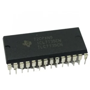
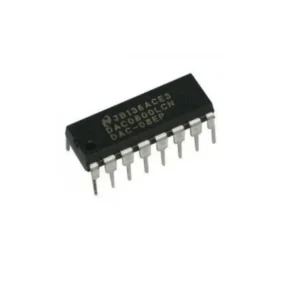
* product image for illustration purposes only. actual product may vary.

There are no reviews yet.