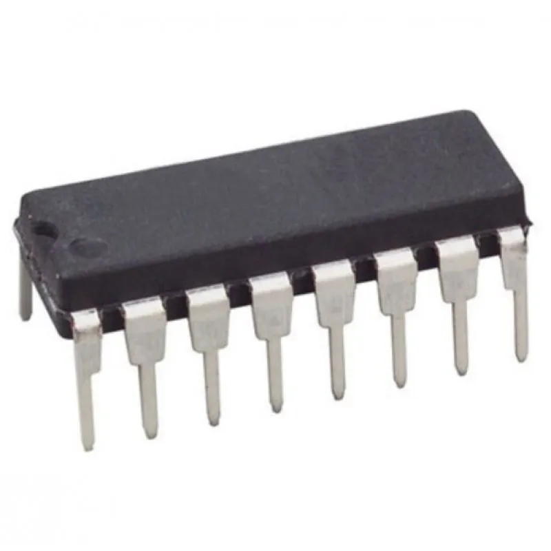
CD4504 hex voltage level-shifter consists of six circuits which shift input signals from the VCC logic level to the VDD logic level. To shift TTL signals to CMOS logic levels, the SELECT input is at the VCC HIGH logic state. When the SELECT input is a LOW logic state, each circuit translates signals from one CMOS level to another.
The CD4504 types are supplied in 16-lead hermetic dual-in-line ceramic packages (F3A suffix), 16-lead dual-in-line plastic packages (E suffix), 16-lead small-outline packages (M, M96, and MT suffixes), and 16-lead thin shrink small-outline packages (PW and PWR suffixes).
Features:-
- Independence of power-supply sequence considerations – VCC can exceed VDD; input signals can exceed both VCC and VDD
- Up and down level-shifting capability
- Shiftable input threshold for either CMOS or TTL compatibility
- Standardized symmetrical output characteristics
- 100% tested for quiescent current @ 20 V
- Maximum input current of 1 µA at 18 V over full package-temperature range; 100 nA at 18 V and 25°C
- 5V, 10 V, and 15 V parametric ratings
- Meets all requirements of JEDEC Standard No. 13B, “Standard Specifications for Description of ’B’ Series CMOS Devices”
Specifications:-
| Parameter | Specification |
| Part number | CD4504 |
| Technology Family | CD4000 |
| Bits (#) | 6 |
| Voltage (Nom) (V) | 5 |
| F @ nom voltage (Max) (MHz) | 50 |
| ICC @ nom voltage (Max) (mA) | 0.001 |
| IOL (Max) (mA) | 6.8 |
| IOH (Max) (mA) | -6.8 |
| Schmitt trigger | No |
| tpd @ nom Voltage (Max) (ns) | 2.9 |
| Rating | See Data Sheet |
| Package Group | PDIP|16 |
* product image for illustration purposes only. actual product may vary.


There are no reviews yet.