
CD4011 NAND gates provide the system designer with direct implementation of the NAND function and supplement the existing family of CMOS gates. All inputs and outputs are buffered.
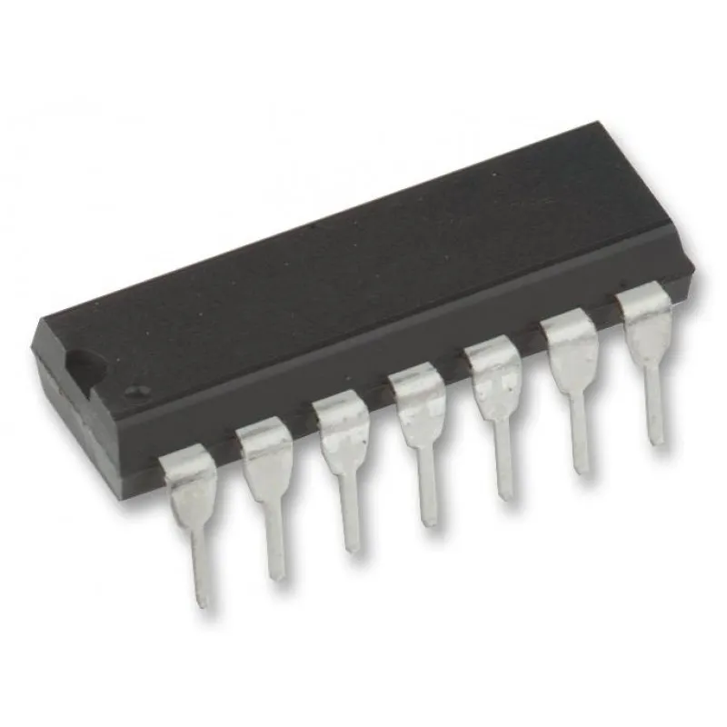
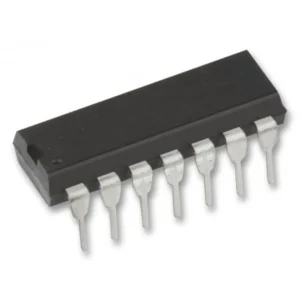
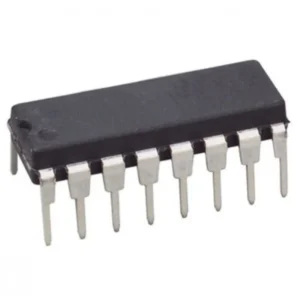
The CD4011 type are supplied in 14-lead hermetic dual-in-line ceramic packages (F3A suffix), 14-lead dual-in-line plastic packages (E suffix), 14-lead small-outline packages (M, MT, M96, and NSR suffixes), and 14-lead thin shrink small-outline packages (PWR suffix). The CD4011 type also are supplied in 14-lead thin shrink small-outline packages (PW suffix).
Features:-
- Propagation delay time = 60 ns (typ.) at CL = 50 pF, VDD = 10 V
- Buffered inputs and outputs
- Standardized symmetrical output characteristics
- Maximum input current of 1 µA at 18 V over-full package temperature range; 100 nA at 18 V and 25°C
- 100% tested for quiescent current at 20 V
- 5-V, 10-V, and 15-V parametric ratings
- Noise margin (over full package temperature range:
1 V at VDD = 5 V
2 V at VDD = 10 V
2.5 at VDD = 15 V - Meets all requirements of JEDEC Tentative Standard No. 13B, “Standard Specifications for Description of “B” Series CMOS Devices”.
Specifications:-
| Parameter | Specification |
| Part number | CD4011B |
| Technology Family | CD4000 |
| VCC (Min) (V) | 3 |
| VCC (Max) (V) | 18 |
| Channels (#) | 4 |
| Inputs per channel | 2 |
| IOL (Max) (mA) | 6.8 |
| IOH (Max) (mA) | -6.8 |
| Input type | Standard CMOS |
| Output type | Push-Pull |
| Features | Standard Speed (tpd > 50ns) |
| Rating | See Data Sheet |
| Data rate (Max) (Mbps) | 8 |
| Operating temperature range (C) | -55 to 125 |
* product image for illustration purposes only. actual product may vary.


There are no reviews yet.