The L4974A is a step down monolithic power switching regulator delivering 3.5A at a voltage variable from 5.1 to 40V. Realized with BCD mixed technology, the device uses a DMOS output transistor to obtain very high efficiency and very fast switching times. Features of the L4974A include reset and power fail for microprocessors, feed forward line regulation, soft start, limiting current and thermal protection. The device is mounted in a Power dip 16 + 2 + 2 plastic package and requires few external components. Efficient operation at switching frequencies up to 200KHz allows reduction in the size and cost of external filter component.
Features:-
• 3.5a Output Current
• 5.1v To 40v Output Voltage Range
• 0 To 90% Duty Cycle Range
• Internal Feed-Forward Line Reg
• Internal Current Limiting
• Precise 5.1v ± 2% On Chip Reference
• Reset And Power Fail Functions .Input/Output Sync Pin
• Under Voltage Lock Out With Hysteretic Turn-On
• Pwm Latch For Single Pulse Per Period
• Very High Efficiency
• Switching Frequency Up To 200khz
• Thermal Shutdown
• Continuous Mode Operation
Specifications:-
| Symbol | Parameters | Values | Units |
| V11 | Input Voltage | 55 | V |
| V11 | Input Operating Voltage | 50 | V |
| V20 | Output DC Voltage | -1 | V |
| Output Peak Voltage at t = 0.1µs f = 200KHz | -7 | ||
| I20 | Maximum Output Current | Internally Limited | |
| V1 | Bootstrap Voltage | 65 | V |
| Bootstrap Operating Voltage | V11 + 15 | ||
| V4, V8 | Input Voltage at Pins 3, 12 | 12 | V |
| V3 | Reset Output Voltage | 50 | V |
| I3 | Reset Output Sink Current | 50 | mA |
| V2, V7, V9, V10 | Input Voltage at Pin 2,7,9,10 | 7 | V |
| I2 | Reset Delay Sink Current | 30 | mA |
| I7 | Error Amplifier Output Sink Current | 1 | A |
| I8 | Soft Start Sink Current | 30 | mA |
| Ptot | Total Power Dissipation at Tcase < 90°C | 5 | W |
| Tj, Tstg | Junction and Storage Temperature | -40 to 150 | °C |
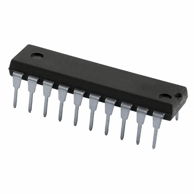
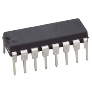
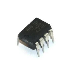
* product image for illustration purposes only. actual product may vary.


There are no reviews yet.