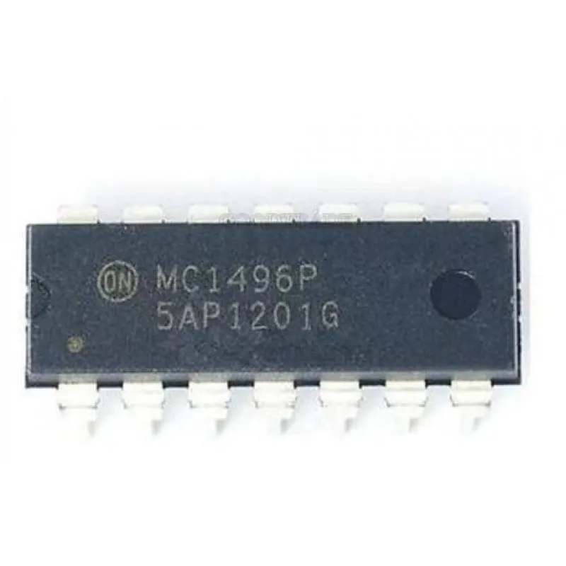
These devices were designed for use where the output voltage is a product of an input voltage (signal) and a switching function (carrier). Typical applications include the suppressed carrier and amplitude modulation, synchronous detection, FM detection, phase detection, and chopper applications. See ON Semiconductor Application Note AN531 for additional design information.
Features:-
- Excellent Carrier Suppression: −65 dB typ @ 0.5 MHz, −50 dB typ @ 10 MHz
- Adjustable Gain and Signal Handling
- Balanced Inputs and Outputs
- High Common Mode Rejection −85 dB Typical
- This Device Contains 8 Active Transistors
- Pb−Free Package is Available
Specification:-
| Parameter | Value |
| Applied Voltage | 30 V |
| Differential Input Signal | 5 V |
| Maximum Bias Current | 10 mA |
| Thermal Resistance, Junction−to−Air Plastic Dual In−Line Package | 100 °C/W |
| Operating Ambient Temperature Range | 0 to +70°C |
| Storage Temperature Range | −65 to +150°C |
| Human Body Model (HBM), Machine Model (MM) | 2000V, 400V |
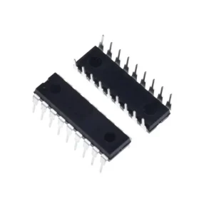
* product image for illustration purposes only. actual product may vary.

There are no reviews yet.