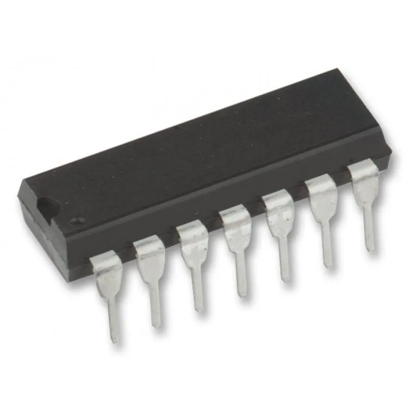
CD4093 consists of four Schmitt-trigger circuits. Each circuit functions as a two-input NAND gate with Schmitt-trigger action on both inputs. The gate switches at different points for positive- and negative-going signals. The difference between the positive voltage (VP) and the negative voltage (VN) is defined as hysteresis voltage (VH) (see Fig. 2).
The CD4093 types are supplied in 14-lead hermetic dual-in-line ceramic packages (F3A suffix), 14-lead dual-in-line plastic packages (E suffix), 14-lead small-outline packages (M, MT, M96, and NSR suffixes), and 14-lead thin shrink small-outline packages (PW and PWR suffixes).
Features:-
- Schmitt-trigger action on each input with no external components
- Hysteresis voltage typically 0.9 V at VDD = 5 V and 2.3 V at VDD = 10 V
- Noise immunity greater than 50%
- No limit on input rise and fall times
- Standardized, symmetrical output characteristics
- 100% tested for quiescent current at 20 V
- Maximum input current of 1 µA at 18 V over full package-temperature range, 100 nA at 18 V and 25°C
- 5-V, 10-V, and 15-V parametric ratings
- Meets all requirements of JEDEC Tentative Standard No. 13B, “Standard Specifications for Description of ‘B’ Series CMOS Devices”
- Applications:
- Wave and pulse shapers
- High-noise-environment systems
- Monostable multivibrators
- Astable multivibrators
- NAND logic
Specifications:-
| Parameter | Specification |
| Part number | CD4093B |
| Technology Family | CD4000 |
| VCC (Min) (V) | 3 |
| VCC (Max) (V) | 18 |
| Channels (#) | 4 |
| Inputs per channel | 2 |
| Input type | Schmitt-Trigger |
| Output type | Push-Pull |
| Features | Standard Speed (tpd > 50ns) |
| Data rate (Max) (Mbps) | 8 |
| IOL (Max) (mA) | 6.8 |
| IOH (Max) (mA) | -6.8 |
| Package size: mm2:W x L (PKG) | 14PDIP: 181 mm2: 9.4 x 19.3 (PDIP|14) |
| Rating | See Data Sheet |
| Operating temperature range (C) | -55 to 125 |
| Package Group | PDIP|14 |
* product image for illustration purposes only. actual product may vary.


There are no reviews yet.